Home
![]()
- Introduction
- Installation in Icestudio
- Shift registers
-
Shift Right registers (SR)
- System Shift right registers (Sys-SR)
- System Shift right registers with reset (Sys-SR-rst)
- System Shift Right with load (Sys-SR-ld)
- System Shift Right with load and reset (Sys-SR-ld-rst)
- Standard Shift right register (SR)
- Standard Shift right register with reset (SR-rst)
- Standard Shift right register with load (SR-ld)
- Standard shift right register with load and reset (SR-ld-rst)
-
Shift Left registers (SL)
- System Shift Left Registers (Sys-SL)
- System Shift Left registers with reset (Sys-SL-rst)
- System Shift Left registers with load (Sys-SL-ld)
- System Shift Left registers with load and reset (Sys-SL-ld-rst)
- Standard Shift Left Register (SL)
- Standard Shift Left Register with reset (SL-rst)
- Standard Shift Left register with load (SL-ld)
- Standard Shift Left register with load an reset (SL-ld-rst)
-
Shift Left Right register (SLR)
- System Shift Left Right Register (Sys-SLR)
- System Shift Left Right register with reset (Sys-SLR-rst)
- System Shift Left Right registers with load (Sys-SLR-ld)
- System Shift left Right registers with load and reset (Sys-SLR-ld-rst)
- Standad Shift Left Right register (SLR)
- Standar Shift Left Right register (SLR-rst)
- Standard Shift Left Right register with load (SLR-ld)
- Standard Shift Left Right register with load and reset
- TestBenches
- Generation scripts
- Translations
- Organization of the collection
- Contributing to the collection
In this collection you will find Shift Registers. Use these blocks in your digital circuits for opensource FPGAs created with icestudio

Find information about collections and how to install them on this link: Installing the iceK collection in Icestudio. It was written for the iceK collection as an example. Use the repo of the iceFF collection instead
- Download the ZIP file from the latest release
- ...or get the ZIP file with the latest changes from the main branch: iceSRegs.zip
The Shift Registers behave like normal registers: They store N-bits of information during a period of time. The data stored (N bits) can be shifted one bit to the right or to the left. There are many flavours:
- Shift to the right, Shift to the left and Shift to the left/right (l/r input)
- System Shift Registers and standard shift registers (shift input)
- With or without load input. These register can load a value and shift it to the left or to the right
- With or without reset input. The reset input stores the default/init value
The SR register shifts its value one bit to the right. All the flavours have an arrow pointing to the right at the top. In this figure the 8 flavours for the 2-bits Shift Right register are shown:

The system shift right register (Sys-SR) shifts its N-bits value one bit to the right on every clock cycle. Therefore, this component is all the time Shifting to the right, at the system clock frecuency (very fast)

The Most significant bit (MSb) is read from the si (serial input) signal and the Least significant bit (lsb) is output to the so pin. The top blue arrow indicates the direction of the shift: to the right
An N-bits system right register is implemented by connecting N flip-flops in cascade. If we want to implement for example an 8-bit shift register to the right in Icestudio, we need to place 8 system flip-flops in a row and connect the output of one flip-flop to the input of the next one. This operation is very simple and easy but it does not scale well. If we want to expand it to a 32-bit shift register, for example, we need to add and connect 24 more flip-flops... it is time consuming
That is the reason why the main implementation of these register is done in verilog. But for shift registers with few bits you will find two more equivalent implementations using Icestudio blocks:
- Implementation 1: It uses system registers (sys-regs) and a combinational shift to the right block
- Implementation 2: It uses system flip-flops (sys-DFF) connected in cascade
If you just want to use the system shift registers for your projects, it is recommended the verilog implementation (the default). For education purposes you can study and modify the other implementations (block implementations)
This is the verilog implementation of the 2-bits Sys-SR block

The verilog code is shown below:
//-- Generic Shift Right
//-- System register
//-- Number of bits
localparam N = 2;

//-- Initial value
reg [N-1:0] qi = INI;

always @(posedge clk)
begin
  //-- Shift to the right
  qi <= {sin,q[N-1:1]};
end

//-- Serial out:
//-- It is the least significant bit
assign sout = qi[0];

//-- Paralell out
assign q = qi;
The code is generic for an N-bits System shift right register. The only difference is the value of the N parameter and the size of the ports in the Icestudio block
This is an implementation using only Icestudio blocks (no verilog code). The 2 bits Sys-SR block is implemented from a 2-bits system registers and a Combinational Shift right block

More information about these blocks in the following links:
- Iceswires collection: Combinational Shift block
- IceReg collection: system registers
This is an implementation using only Icestudio blocks (no verilog code). The 2 bits Sys-SR block is implemented connecting two system DFF in cascade. This implementation is equivalent to the other two previous implementations

The two bits unary counter starts with the initial value 00, then 10 and finally 11. This value is stable and the counter will not change anymore until the board is reset. This chronogram shows the values of the register in all the cycle clocks:

This unary counter is very esily implemented using a 2-bits system shift right register with its si input connected to 1

As this is a system register, it counts very fast (at the system clock rate of speed). To check that it is working properly we need to meassure its output using a data ledoscope. It captures the register data for 4 clocks. The current sample is shown on the LEDs. Using the sw1 button the next sample is shown

Implementation of an 8-bits unary counter that counts from 1 (10000000) to 8 (11111111). This is the cronogram:

This is the circuit. It is implemented using an 8-bits System shift right register with an initial value 0f 0x80 (10000000 in binary):

The register output is connected to an 8-bits data-Osciloscope. Only 8 samples are taken. Using the button SW1 the register values captured are displayed on the LEDs. This is the complete example:

The System Shift Right register with reset (Sys-SR-rst) works exactly the same as the Sys-SR: it shifts the register value one bit to the right on every clock cycle. But it includes the rst input for setting the register to its initial value (The one set in their Init top parameter)

This is the verilog implementation of the 2-bits Sys-SR-rst block

The verilog code is shown below:
//-- Generic Shift Right
//-- System register with reset
//-- Number of bits
localparam N = 2;

//-- Initial value
reg [N-1:0] qi = INI;

always @(posedge clk)
begin

  //-- Reset
  if (rst==1)
    //-- Capture initial value
    qi <= INI;
  else
    //-- Shift to the right
    qi <= {sin,qi[N-1:1]};
end

//-- Serial out:
//-- It is the least significant bit
assign sout = qi[0];

//-- Paralell out
assign q = qi;
The reset signal has the highest priority. When reset is 1, the register is loaded with its initial value (and no shift is performed). It will only shift to the right if reset is 0
This is an implementation using only Icestudio blocks (no verilog code). The 2 bits Sys-SR-rst block is implemented from a 2-bits system registers with reset and a Combinational Shift right block

More information about these blocks in the following links:
- Iceswires collection: Combinational Shift block
- IceReg collection: system registers
This is an implementation using only Icestudio blocks (no verilog code). The 2 bits Sys-SR-rst block is implemented connecting two system DFF with reset in cascade. This implementation is equivalent to the other two previous implementations

Implementation of an 2-bits unary counter that counts from 0 (00) to 3 (11) and then start it again. This is the cronogram:

When the reset signal is set, the counter loads its initial 00 value
This is the circuit. It is implemented using a 2-bits System shift right register with reset. The initial value is 00

The register's least significant bit is used as the reset signal. When the register get the 11 value, the reset is active and it will load 00 in the next clock cycle, starting the count again
The register output is connected to an 8-bits data-Osciloscope. Only 8 samples are taken. Using the button SW1 the register values captured are displayed on the LEDs. This is the complete example:

The System Shift Right register with load (Sys-SR-ld) works exactly the same as the Sys-SR: it shifts the register value one bit to the right on every clock cycle. But it includes the load input for loading the external value located in its data input (d)

The load signal has the highest priority. When it is active (1), the register does not perform the shifting. The shifting is done on every clock cycle only done when load is NOT active (0)
This is the verilog implementation of the 3-bits Sys-SR-ld block

The verilog code is shown below:
//-- Generic Shift Right
//-- System register with reset
//-- Number of bits
localparam N = 3;

//-- Initial value
reg [N-1:0] qi = INI;

always @(posedge clk)
begin

  //-- Load
  if (load==1)
    //-- Capture the value
    qi <= d;
  else
    //-- Shift to the right
    qi <= {sin,q[N-1:1]};
end

//-- Serial out:
//-- It is the least significant bit
assign sout = qi[0];

//-- Paralell out
assign q = qi;
It can be seen that load has the highest priority: it is the first condition checked. If not active, then the shifting is performed
This is an implementation using only Icestudio blocks (no verilog code). The 2 bits Sys-SR-rst block is implemented from a 2-bits system registers a Combinational Shift right block and a 2-bits 2-1 Mux

The system register is all the time capturing data from its input. The Mux is in charge of selecting which data is going to be loaded: either the external data or the shifted value. This selection is controlled by the load signal. When it is 1, the Mux select the external data (d input). When it is 0, the shifted data (sdata) is used instead
More information about these blocks in the following links:
- Iceswires collection: Combinational Shift block
- IceReg collection: system registers
- IceMux collection: Muxes
This is an implementation using only Icestudio blocks (no verilog code). The 2 bits Sys-SR-ld block is implemented connecting two system DFFs with load in cascade

The load signal is connected directly to the load input of the Systems DFFs. They can either load the value from their si input (when load is 0) or from their d input when load is 1
This implementation is equivalent to the other two previous implementations
A typical application of the shift registers is to convert a number of N-bits (N bits in paralell) to serial. It is used for implementing Synchronous/asyncronous serial transmitters (Serial port, I2C bus, SPI...)
In this example, two 3-bit values are converted to serial by sifthing to the right. The first value is loaded on cycle 1 and the next on cycle 4. The evolution of the register data and its load signal is shown on the following chronogram. The values converted to serial are 101 and 111:

Initially (cycle 0) the register has the value 000. As the load signal is active on cycle 0, when the rising edge of the clock arrives, the value 101 is loaded. It value remains stable during cycle 1. In the next cycles the value is shifted to the right (the least significant bit contains the data in serial). The load input is actived again on cycle 3, so that the value 111 is loaded and available on cycle 4. This new value is then shifted to the right (as load is 0)
This circuit is divided into two main parts: the datapath and the controller. The Datapath contains the System shift right register and the two values to be converted to serial:

This Datapaht is controlled by the signals cycle0 and cycle3 generated by the controller. These signals are only active on cycles 0 and 3 respectivelly. Therefore, the union of the two signals (or gate) indicates when a new value should be loaded into the shift register
This controller is implemented using a 4-bit System shift right register initialized with the value 1000. The most significant bit is the signal cycle0 and the least significant bit is the cycle3 signal

As always, the register output is connected to an 8-bits data-Osciloscope. Only 8 samples are taken. Using the button SW1 the register values captured are displayed on the LEDs. This is the complete example:

Shif registers can be used to perform the opposite operation: conversion from serial to paralell. It allows us to implement serial receivers. The bits enter to the register one at a time, and the result is shown in paralell
In this example the 3-bit values 101 (value 1) and 111 (value 2) are sent serially to a receiver register that convert them to paralell. The values are stored in two different registers: Reg1 and Reg2 that display the values 1 and 2 respectivelly on the LEDs

Initially the rx register has the value 000. It receives the serial bits. On cycle 3 the first value (101) has been received and it is stored in register 1. On cycle 6 the second value (111) is received and stored in register 2
The serial transmisión is performed by two 3-bit system shift right registers in cascade, initialized with the values 1 and 2. These two registers are equivalent to one 6-bit system shift right register
The serial bits enter into a 3-bits system shift right register with load though its serial input (si). As the load input is not used, this register is equivalent to a system shift right register

This circuit is divided into two main parts: the datapath and the controller. The Datapath contains the transmitter and the receiver, as well as the register 1 and 2 that stored the received values: value 1 and value 2. These registers are loaded when the signals cycle3 and cycle6 are activated by the controller

This controller is implemented using a 7-bit System shift right register initialized with the value 1000_000. Its bit 3 is the signal cycle3 that controlls when the register 1 is loaded (on cycle 3) and the bit 0 (cycle6) controlls when the register 2 is loaded

As always, the RX register output is connected to an 8-bits data-Osciloscope. Only 8 samples are taken. Using the button SW1 the register values captured are displayed on the LEDs. This is the complete example:

Another typicall aplication of the shift registers is to perform arithmetics operations one bit at a time (serially). It saves resources, but takes longer to execute
In this example the addition of the numbers 5 and 7 is done using a full adder. The bits of the two numbers are sifthed to the full adder. The carry of the previous operation is stored in a system DFF

The rest of the circuit is quite similar to the example 5. The output of the adder is sent serially to a system shift right register converting to a paralell value that is then capture by a another system registers, and the number displayed on the leds

The controller generates the load signal on cycle 4:

This is the complete example:

The System Shift Right register with load and reset (Sys-SR-ld-rst) works exactly the same as the Sys-SR-ld: it shifts the register value one bit to the right on every clock cycle, and it loads the external values. In addition, it includes the reset input that set the register to its initial value
The reset signal has the highest priority. Then the load signal and finally the shifting. The shifting is done on every clock cycle only done when load and rst are NOT active (0)
This is the verilog implementation of the 3-bits Sys-SR-ld-rst block

The verilog code is shown below:
//-- Generic Shift Right
//-- System register with reset
//-- Number of bits
localparam N = 3;

//-- Initial value
reg [N-1:0] qi = INI;

always @(posedge clk)
begin

  //-- reset
  if (rst==1)
    qi <= INI;

  else
    //-- Load
    if (load==1)
      //-- Capture the value
      qi <= d;
    else
      //-- Shift to the right
      qi <= {sin,q[N-1:1]};
end

//-- Serial out:
//-- It is the least significant bit
assign sout = qi[0];

//-- Paralell out
assign q = qi;
It can be seen that reset has the highest priority: it is the first condition checked. If not active, then the load is checked. And finally, the shifting is performed
This is an implementation using only Icestudio blocks (no verilog code). The 2 bits Sys-SR-ld-rst block is implemented from a 2-bits system registers with reset a Combinational Shift right block and a 2-bits 2-1 Mux

The system register is all the time capturing data from its input. The Mux is in charge of selecting which data is going to be loaded: either the external data or the shifted value. This selection is controlled by the load signal. When it is 1, the Mux select the external data (d input). When it is 0, the shifted data (sdata) is used instead
More information about these blocks in the following links:
- Iceswires collection: Combinational Shift block
- IceReg collection: system registers
- IceMux collection: Muxes
This is an implementation using only Icestudio blocks (no verilog code). The 2 bits Sys-SR-ld-rst block is implemented connecting two system DFFs with load and reset in cascade

The load and reset signals are connected directly to the load and reset input of the Systems DFFs. They can either load the value from their si input (when load is 0) or from their d input when load is 1
This implementation is equivalent to the other two previous implementations
The standard shift right register (SR) or simply shift right register shifts its N-bits value one bit to the right when its shift input is active. If one cycle pulse is applied to this input, the value is shifted 1-bit to the right. If the shift input remains active, it behaves exactly the same as the system shift right register (Shifting the value on every clock cycle)
As the shifting is controlled by the shift input, it allows us to shift the data at any rate of speed less than (or equal to) the system clock. Therefore these are the shift registers used for implementing serial transmiter/receivers with configurable speed

The Most significant bit (MSb) is read from the si (serial input) signal and the Least significant bit (lsb) is output to the so pin. The top blue arrow indicates the direction of the shift: to the right
This is the verilog implementation of the 2-bits SR block

The verilog code is shown below:
//-- Generic Shift Right register
//-- Number of bits
localparam N = 3;

//-- Initial value
reg [N-1:0] qi = INI;

always @(posedge clk)
begin

  //-- Shift to the right when the
  //-- shift iput is 1
  if (shift == 1)

    //-- Shift to the right
    qi <= {sin,qi[N-1:1]};
end

//-- Serial out:
//-- It is the least significant bit
assign sout = qi[0];

//-- Paralell out
assign q = qi;This is an implementation using only Icestudio blocks (no verilog code). The 2 bits SR block is implemented from a 2-bits register with load and a Combinational Shift right block. The shift input is connected to the register's load input

More information about these blocks in the following links:
- Iceswires collection: Combinational Shift block
- IceReg collection: Registers
This is an implementation using only Icestudio blocks (no verilog code). The 2 bits SR block is implemented connecting two DFFs in cascade. This implementation is equivalent to the other two previous implementations

Example of an unary counter that counts from 0 to 1111 (4). The counter is increased by 1 when the button is pressed

The Shift Right register with reset (SR-rst) works exactly the same as the SR: it shifts the register value one bit to the right when the shift input is 1. But it includes the rst input for setting the register to its initial value (The one set in their Init top parameter)

This is the verilog implementation of the 2-bits SR-rst block

The verilog code is shown below:
//-- Generic Shift Right register
//-- With reset input
//-- Number of bits
localparam N = 2;

//-- Initial value
reg [N-1:0] qi = INI;

always @(posedge clk)
begin

  //-- Reset
  if (rst == 1)
    qi <= INI;

  else
    //-- Shift to the right when the
    //-- shift iput is 1
    if (shift == 1)

      //-- Shift to the right
      qi <= {sin,qi[N-1:1]};
end

//-- Serial out:
//-- It is the least significant bit
assign sout = qi[0];

//-- Paralell out
assign q = qi;
The reset signal has the highest priority. When reset is 1, the register is loaded with its initial value. If reset is 0 then the shift input is checked. It will shift to the right if it is set (and reset is 0)
This is an implementation using only Icestudio blocks (no verilog code). The 2 bits SR-rst block is implemented from a 2-bits registers with load and reset and a Combinational Shift right block

More information about these blocks in the following links:
- Iceswires collection: Combinational Shift block
- IceReg collection: Registers
This is an implementation using only Icestudio blocks (no verilog code). The 2 bits SR-rst block is implemented connecting two DFF with reset in cascade. This implementation is equivalent to the other two previous implementations

Example of an unary counter that counts from 0 to 1111 (4) and start it again from 0. The counter is increased every second

The reset input allow us to implement repetitive behaviours
The Shift Right register with load (SR-ld) works exactly the same as the SR: it shifts the register value one bit to the right when the shift input is set. But it includes the load input for loading the external value located in its data input (d) (It is also called parallel input)

The load signal has the highest priority. When it is active (1), the register does not perform the shifting. The shifting is done when the shift input is 1 and the load is NOT active (0)
This is the verilog implementation of the 2-bits SR-ld block

The verilog code is shown below:
//-- Generic Shift Right register
//-- With reset input
//-- Number of bits
localparam N = 2;

//-- Initial value
reg [N-1:0] qi = INI;

always @(posedge clk)
begin

  //-- Load
  if (load == 1)
    qi <= din[1:0];

  else
    //-- Shift to the right when the
    //-- shift iput is 1
    if (shift == 1)

      //-- Shift to the right
      qi <= {sin,qi[N-1:1]};
end

//-- Serial out:
//-- It is the least significant bit
assign sout = qi[0];

//-- Paralell out
assign q = qi;
The load signal has the highest priority. When load is 1, the register is loaded with the external data. If load is 0 then the shift input is checked. It will shift to the right if it is set (and load is 0)
This is an implementation using only Icestudio blocks (no verilog code). The 2 bits SR-ld block is implemented from a 2-bits registers, a Combinational Shift right block and a 2-1 Mux

More information about these blocks in the following links:
- Iceswires collection: Combinational Shift block
- IceReg collection: Registers
- IceMux collection: Mux 2-1
This is an implementation using only Icestudio blocks (no verilog code). The 2 bits SR-ld block is implemented connecting two DFFs in cascade with two 2-1 Muxex. This implementation is equivalent to the other two previous implementations

This is an example of the serial transmision of a 4-bits data (0xa) from the transmitter to the receiver at the rate of speed of 1 bit per second
The circuit is divided in four parts:
-
Timming generator: It generates que
tiksignal every second. It is the clock used for the transmission/reception. When this signal is active (every second) theLED7is toggled, for debugging purposes -
Transmitter: It transmits the data
0xa. Converts from parallel to serial - Receiver: It receives the data and stores it in a 4-bit register. Serial to parallel conversion
- Controller: It generates the control signals that perform the needed actions on the transmitter/receiver
The timming generator is implemented by the heart-tic-hz from the iceheart collection

The transmitter is implemented by a SR-ld register that loads the paralell data 0xa. The current value of this register is shown on the LEDs

The receiver is implemented by two register. The first one is connected to the serial line and converts from serial to paralell. The second one is for storing the received data

The controller is in charge of generating the signals load, shift and rx:
-
load: It is generated initially for loading the data to transfer -
shift: It shifts both the receiver and transmitter registers -
rx: It is generated in the end for capturing the received data

This is the complete example:

The Shift Right register with load and reset (SR-ld-rst) works exactly the same as the SR-ld, but it includes the reset input for restoring the initial value

The reset signal has the highest priority. When it is active (1), the register loads its initial value. The load signal has the next priority. It only works if reset is not active. Finally, the less priority is for the shift signal. It only works if both reset and load are inactive
This is the verilog implementation of the 2-bits SR-ld-rst block

The verilog code is shown below:
//-- Generic Shift Right register
//-- With load and reset input
//-- Number of bits
localparam N = 2;

//-- Initial value
reg [N-1:0] qi = INI;

always @(posedge clk)
begin

  //-- Reset has the higher priority
  if (rst == 1)
    qi <= INI;

  else
    //-- Load
    if (load == 1)
      qi <= din[1:0];

    else
      //-- Shift to the right when the
      //-- shift input is 1
      if (shift == 1)

        //-- Shift to the right
        qi <= {sin,qi[N-1:1]};
end

//-- Serial out:
//-- It is the least significant bit
assign sout = qi[0];

//-- Paralell out
assign q = qi;
This implementation shows clearly the signals priority: the high priority por the reset signal, then load and shift with the lowest priority
This is an implementation using only Icestudio blocks (no verilog code). The 2 bits SR-ld block is implemented from a 2-bits registers, a Combinational Shift right block and a 2-1 Mux

More information about these blocks in the following links:
- Iceswires collection: Combinational Shift block
- IceReg collection: Registers
- IceMux collection: Mux 2-1
This is an implementation using only Icestudio blocks (no verilog code). The 2 bits SR-ld-rst block is implemented connecting two DFFs with reset in cascade with two 2-1 Muxex. This implementation is equivalent to the other two previous implementations

The SL register shifts its value one bit to the left. All the flavours have an arrow pointing to the left at the top. In this figure the 8 flavours for the 2-bits Shift left register are shown:

The system shift left register (Sys-SL) shifts its N-bits value one bit to the left on every clock cycle. Therefore, this component is all the time Shifting to the left, at the system clock frecuency (very fast)

The Least significant bit (lsb) is read from the si (serial input) signal and the Most significant bit (MSb) is output to the so pin. The top blue arrow indicates the direction of the shift: to the left
An N-bits system left register is implemented by connecting N flip-flops in cascade. If we want to implement for example an 8-bit shift register to the left in Icestudio, we need to place 8 system flip-flops in a row and connect the output of one flip-flop to the input of the next one. As in icestudio inputs are located on the left and outputs on the right, labels are used for the connections. This operation is very simple and easy but it does not scale well. If we want to expand it to a 32-bit shift register, for example, we need to add and connect 24 more flip-flops... (along with their labels) it is time consuming
That is the reason why the main implementation of these register is done in verilog. But for shift registers with few bits you will find two more equivalent implementations using Icestudio blocks:
- Implementation 1: It uses system registers (sys-regs) and a combinational shift to the right block
- Implementation 2: It uses system flip-flops (sys-DFF) connected in cascade
If you just want to use the system shift registers for your projects, it is recommended the verilog implementation (the default). For education purposes you can study and modify the other implementation (block implementations)
This is the verilog implementation of the 2-bits Sys-SL block

The verilog code is shown below:
//-- Generic Shift Left
//-- System register
//-- Number of bits
localparam N = 2;

//-- Initial value
reg [N-1:0] qi = INI;

always @(posedge clk)
begin
  //-- Shift to the left
  qi <= {qi[N-2:0], sin};
end

//-- Serial out:
//-- It is the most significant bit
assign sout = qi[N-1];

//-- Paralell out
assign q = qi;
The code is generic for an N-bits System shift left register. The only difference is the value of the N parameter and the size of the ports in the Icestudio block
This is an implementation using only Icestudio blocks (no verilog code). The 2 bits Sys-SL block is implemented from a 2-bits system registers and a Combinational Shift left block

More information about these blocks in the following links:
- Iceswires collection: Combinational Shift block
- IceReg collection: system registers
This is an implementation using only Icestudio blocks (no verilog code). The 2 bits Sys-SL block is implemented connecting two system DFF in cascade. This implementation is equivalent to the other two previous implementations

The System Shift Left register with reset (Sys-SL-rst) works exactly the same as the Sys-SL: it shifts the register value one bit to the left on every clock cycle. But it includes the rst input for setting the register to its initial value (The one set in their Init top parameter)

This is the verilog implementation of the 2-bits Sys-SL-rst block

The verilog code is shown below:
//-- Generic Shift Left
//-- System register
//-- Number of bits
localparam N = 2;

//-- Initial value
reg [N-1:0] qi = INI;

always @(posedge clk)
begin
  //-- Reset
  if (rst==1)
    //-- Capture initial value
    qi <= INI;
  else
    //-- Shift to the left
    qi <= {qi[N-2:0], sin};
end

//-- Serial out:
//-- It is the most significant bit
assign sout = q[N-1];

//-- Paralell out
assign q = qi;
The reset signal has the highest priority. When reset is 1, the register is loaded with its initial value (and no shift is performed). It will only shift to the right if reset is 0
This is an implementation using only Icestudio blocks (no verilog code). The 2 bits Sys-SL-rst block is implemented from a 2-bits system registers with reset and a Combinational Shift left block

More information about these blocks in the following links:
- Iceswires collection: Combinational Shift block
- IceReg collection: system registers
This is an implementation using only Icestudio blocks (no verilog code). The 2 bits Sys-SL-rst block is implemented connecting two system DFF with reset in cascade. This implementation is equivalent to the other two previous implementations

The System Shift Left register with load (Sys-SL-ld) works exactly the same as the Sys-SL: it shifts the register value one bit to the left on every clock cycle. But it includes the load input for loading the external value located in its data input (d)

The load signal has the highest priority. When it is active (1), the register does not perform the shifting. The shifting is done on every clock cycle when load is NOT active (0)
This is the verilog implementation of the 3-bits Sys-SL-ld block

The verilog code is shown below:
//-- Generic Shift Left
//-- System register with reset
//-- Number of bits
localparam N = 3;

//-- Initial value
reg [N-1:0] qi = INI;

always @(posedge clk)
begin

  //-- Load
  if (load==1)
    //-- Capture the value
    qi <= d;
  else
    //-- Shift to the left
    qi <= {qi[N-2:0], sin};
end

//-- Serial out:
//-- It is the least significant bit
assign sout = qi[N-1];

//-- Paralell out
assign q = qi;
It can be seen that load has the highest priority: it is the first condition checked. If not active, then the shifting is performed
This is an implementation using only Icestudio blocks (no verilog code). The 2 bits Sys-SL-rst block is implemented from a 2-bits system registers, a Combinational Shift left block and a 2-bits 2-1 Mux

The system register is all the time capturing data from its input. The Mux is in charge of selecting which data is going to be loaded: either the external data or the shifted value. This selection is controlled by the load signal. When it is 1, the Mux select the external data (d input). When it is 0, the shifted data (sdata) is used instead
More information about these blocks in the following links:
- Iceswires collection: Combinational Shift block
- IceReg collection: system registers
- IceMux collection: Muxes
This is an implementation using only Icestudio blocks (no verilog code). The 2 bits Sys-SL-ld block is implemented connecting two system DFFs with load in cascade

The load signal is connected directly to the load input of the Systems DFFs. They can either load the value from their si input (when load is 0) or from their d input when load is 1
This implementation is equivalent to the other two previous implementations
The System Shift Left register with load and reset (Sys-SL-ld-rst) works exactly the same as the Sys-SL-ld: it shifts the register value one bit to the left on every clock cycle, and it loads the external values. In addition, it includes the reset input that set the register to its initial value

The reset signal has the highest priority. Then the load signal and finally the shifting. The shifting is done on every clock cycle only when load and rst are NOT active (0)
This is the verilog implementation of the 2-bits Sys-SL-ld-rst block

The verilog code is shown below:
//-- Generic Shift Left
//-- System register with reset
//-- Number of bits
localparam N = 2;

//-- Initial value
reg [N-1:0] qi = INI;

always @(posedge clk)
begin
  //-- Reset
  if (rst==1)
    //-- Capture initial value
    qi <= INI;
  else
    //-- Load
    if (load==1)
      //-- Capture the value
      qi <= d;
    else
      //-- Shift to the left
      qi <= {qi[N-2:0], sin};
end

//-- Serial out:
//-- It is the least significant bit
assign sout = qi[N-1];

//-- Paralell out
assign q = qi;
It can be seen that reset has the highest priority: it is the first condition checked. If not active, then the load is checked. And finally, the shifting is performed
This is an implementation using only Icestudio blocks (no verilog code). The 2 bits Sys-SL-ld-rst block is implemented from a 2-bits system registers with reset, a Combinational Shift left block and a 2-bits 2-1 Mux

The system register is all the time capturing data from its input. The Mux is in charge of selecting which data is going to be loaded: either the external data or the shifted value. This selection is controlled by the load signal. When it is 1, the Mux select the external data (d input). When it is 0, the shifted data (sdata) is used instead
More information about these blocks in the following links:
- Iceswires collection: Combinational Shift block
- IceReg collection: system registers
- IceMux collection: Muxes
This is an implementation using only Icestudio blocks (no verilog code). The 2 bits Sys-SL-ld-rst block is implemented connecting two system DFFs with load and reset in cascade

The load and reset signals are connected directly to the load and reset input of the Systems DFFs. They can either load the value from their si input (when load is 0) or from their d input when load is 1
This implementation is equivalent to the other two previous implementations
The standard shift left register (SL) or simply shift left register shifts its N-bits value one bit to the left when its shift input is active. If one cycle pulse is applied to this input, the value is shifted 1-bit to the left. If the shift input remains active, it behaves exactly the same as the system shift left register (Shifting the value on every clock cycle)
As the shifting is controlled by the shift input, it allows us to shift the data at any rate of speed less than (or equal to) the system clock. Therefore these shift registers are used for implementing serial transmiter/receivers with configurable speed

The Least significant bit (lsb) is read from the si (serial input) signal and the Most significant bit (MSb) is output to the so pin. The top blue arrow indicates the direction of the shift: to the left
This is the verilog implementation of the 3-bits SL block

The verilog code is shown below:
//-- Generic Shift left register
//-- Number of bits
localparam N = 3;

//-- Initial value
reg [N-1:0] qi = INI;

always @(posedge clk)
begin

  //-- Shift to the left when the
  //-- shift iput is 1
  if (shift == 1)

    //-- Shift to the left
    qi <= {qi[N-2:0], sin};
end

//-- Serial out:
//-- It is the most significant bit
assign sout = qi[N-1];

//-- Paralell out
assign q = qi;This is an implementation using only Icestudio blocks (no verilog code). The 2 bits SL block is implemented from a 2-bits register with load and a Combinational Shift left block. The shift input is connected to the register's load input

More information about these blocks in the following links:
- Iceswires collection: Combinational Shift block
- IceReg collection: Registers
This is an implementation using only Icestudio blocks (no verilog code). The 2 bits SL block is implemented connecting two DFFs in cascade. This implementation is equivalent to the other two previous implementations

The Shift Left register with reset (SL-rst) works exactly the same as the SL: it shifts the register value one bit to the right when the shift input is 1. But it includes the rst input for setting the register to its initial value (The one set in their Init top parameter)

This is the verilog implementation of the 2-bits SL-rst block

The verilog code is shown below:
//-- Generic Shift Left register
//-- With reset input
//-- Number of bits
localparam N = 2;

//-- Initial value
reg [N-1:0] qi = INI;

always @(posedge clk)
begin

  //-- Reset
  if (rst == 1)
    qi <= INI;

  else
    //-- Shift to the right when the
    //-- shift iput is 1
    if (shift == 1)

      //-- Shift to the left
      qi <= {qi[N-2:0], sin};
end

//-- Serial out:
//-- It is the least significant bit
assign sout = qi[N-1];

//-- Paralell out
assign q = qi;
The reset signal has the highest priority. When reset is 1, the register is loaded with its initial value. If reset is 0 then the shift input is checked. It will shift to the right if it is set (and reset is 0)
This is an implementation using only Icestudio blocks (no verilog code). The 2 bits SL-rst block is implemented from a 2-bits registers with reset and a Combinational Shift left block

More information about these blocks in the following links:
- Iceswires collection: Combinational Shift block
- IceReg collection: Registers
This is an implementation using only Icestudio blocks (no verilog code). The 2 bits SL-rst block is implemented connecting two DFF with reset in cascade. This implementation is equivalent to the other two previous implementations

The Shift Left register with load (SL-ld) works exactly the same as the SL: it shifts the register value one bit to the left when the shift input is set. But it includes the load input for loading the external value located in its data input (d) (It is also called parallel input)

The load signal has the highest priority. When it is active (1), the register does not perform the shifting. The shifting is done when the shift input is 1 and the load is NOT active (0)
This is the verilog implementation of the 2-bits SL-ld block

The verilog code is shown below:
//-- Generic Shift Left register
//-- With reset input
//-- Number of bits
localparam N = 2;

//-- Initial value
reg [N-1:0] qi = INI;

always @(posedge clk)
begin

  //-- Load
  if (load == 1)
    qi <= din[1:0];

  else
    //-- Shift to the right when the
    //-- shift iput is 1
    if (shift == 1)

      //-- Shift to the left
      qi <= {qi[N-2:0], sin};
end

//-- Serial out:
//-- It is the most significant bit
assign sout = qi[N-1];

//-- Paralell out
assign q = qi;
The load signal has the highest priority. When load is 1, the register is loaded with the external data. If load is 0 then the shift input is checked. It will shift to the right if it is set (and load is 0)
This is an implementation using only Icestudio blocks (no verilog code). The 2 bits SL-ld block is implemented from a 2-bits registers a Combinational Shift right block and a 2-1 Mux

More information about these blocks in the following links:
- Iceswires collection: Combinational Shift block
- IceReg collection: Registers
- IceMux collection: Mux 2-1
This is an implementation using only Icestudio blocks (no verilog code). The 2 bits SL-ld block is implemented connecting two DFFs in cascade with two 2-1 Muxex. This implementation is equivalent to the other two previous implementations

The Shift Left register with load and reset (SL-ld-rst) works exactly the same as the SL-ld, but it includes the reset input for restoring the initial value

The reset signal has the highest priority. When it is active (1), the register loads its initial value. The load signal has the next priority. It only works if reset is not active. Finally, the less priority is for the shift signal. It only works if both reset and load are inactive
This is the verilog implementation of the 2-bits SL-ld-rst block

The verilog code is shown below:
//-- Generic Shift Left register
//-- With load and reset input
//-- Number of bits
localparam N = 2;

//-- Initial value
reg [N-1:0] qi = INI;

always @(posedge clk)
begin

  //-- Reset has the higher priority
  if (rst == 1)
    qi <= INI;

  else
    //-- Load
    if (load == 1)
      qi <= din[1:0];

    else
      //-- Shift to the right when the
      //-- shift input is 1
      if (shift == 1)

        //-- Shift to the left
        qi <= {qi[N-2:0], sin};
end

//-- Serial out:
//-- It is the least significant bit
assign sout = qi[N-1];

//-- Paralell out
assign q = qi;
This implementation shows clearly the signals priority: the high priority por the reset signal, then load and shift with the lowest priority
This is an implementation using only Icestudio blocks (no verilog code). The 2 bits SL-ld-rst block is implemented from a 2-bits registers, a Combinational Shift left block and a 2-1 Mux

More information about these blocks in the following links:
- Iceswires collection: Combinational Shift block
- IceReg collection: Registers
- IceMux collection: Mux 2-1
This is an implementation using only Icestudio blocks (no verilog code). The 2 bits SL-ld-rst block is implemented connecting two DFFs with reset in cascade with two 2-1 Muxex. This implementation is equivalent to the other two previous implementations

The SLR register shifts its value one bit to the left or to the right depending on the input lr. All the flavours have two arrows, one pointing to the left and the other pointing to the right. In this figure the 8 flavours for the 2-bits Shift Left Right register are shown:

The system shift left right register (Sys-SLR) shifts its N-bits value one bit to the left or to the right, depending on its input lr, on every clock cycle. Therefore, this component is all the time Shifting to the right or left, at the system clock frecuency (very fast)

When shifting to the right (lr=0), the Most significant bit (MSB) is read from the MSB input. When shifting to the left (lr=1) the Least significant bit (lsb) is read from the lsb input. The top blue arrows indicate that this register can perform shifts in both directions
An N-bits system left right register is implemented by connecting N flip-flops in cascade. If we want to implement for example an 8-bit shift register to the left or right in Icestudio, we need to place 8 system flip-flops in a row and connect the output of one flip-flop to the input of the next one, by means of multiplexers. This operation is very simple and easy but it does not scale well. If we want to expand it to a 32-bit shift register, for example, we need to add and connect 24 more flip-flops... it is time consuming
That is the reason why the main implementation of these register is done in verilog. But for shift registers with few bits you will find two more equivalent implementations using Icestudio blocks:
- Implementation 1: It uses system registers (sys-regs) and a combinational shift to the right block
- Implementation 2: It uses system flip-flops (sys-DFF) connected in cascade
If you just want to use the system shift registers for your projects, it is recommended the verilog implementation (the default). For education purposes you can study and modify the other implementation (block implementations)
This is the verilog implementation of the 2-bits Sys-SLR block

The verilog code is shown below:
//-- Generic Shift Left/Right
//-- System register
//-- Number of bits
localparam N = 2;

//-- Initial value
reg [N-1:0] qi = INI;

always @(posedge clk)
begin

  if (lr == 0)
    //-- Shift to the right
    qi <= {MSB_i,qi[N-1:1]};

  //-- lr == 1
  else
    //-- Shift to the left
    qi <= {qi[N-2:0], lsb_i};
end

//-- Serial out:
//-- Least significant bit
assign lsb_o = qi[0];

//-- most significant bit
assign MSB_o = qi[N-1];

//-- Paralell out
assign q = qi;
The code is generic for an N-bits System shift left right register. The only difference is the value of the N parameter and the size of the ports in the Icestudio block
This is an implementation using only Icestudio blocks (no verilog code). The 2 bits Sys-SLR block is implemented from a 2-bits system registers, a Combinational Shift right block, a Combinational Shift left block and a 2-bits 2-1 multiplexer

More information about these blocks in the following links:
- Iceswires collection: Combinational Shift block
- IceReg collection: system registers
This is an implementation using only Icestudio blocks (no verilog code). The 2 bits Sys-SLR block is implemented connecting two system DFF in cascade. This implementation is equivalent to the other two previous implementations

The System Shift Left Right register with reset (Sys-SLR-rst) works exactly the same as the Sys-SLR: it shifts the register value one bit to the right or left on every clock cycle. But it includes the rst input for setting the register to its initial value (The one set in their Init top parameter)

This is the verilog implementation of the 2-bits Sys-SLR-rst block

The verilog code is shown below:
//-- Generic Shift Left/Right
//-- System register with reset
//-- Number of bits
localparam N = 2;

//-- Initial value
reg [N-1:0] qi = INI;

always @(posedge clk)
begin

  //--Reset (high priority)
  if (rst == 1)

    //-- load initial value
    qi <= INI;

  //-- No reset
  else
    if (lr == 0)
      //-- Shift to the right
      qi <= {MSB_i,qi[N-1:1]};

    //-- lr == 1
    else
      //-- Shift to the left
      qi <= {qi[N-2:0], lsb_i};
end

//-- Serial out:
//-- Least significant bit
assign lsb_o = qi[0];

//-- most significant bit
assign MSB_o = qi[N-1];

//-- Paralell out
assign q = qi;
The reset signal has the highest priority. When reset is 1, the register is loaded with its initial value (and no shift is performed). It will only shift to the right if reset is 0
This is an implementation using only Icestudio blocks (no verilog code). The 2 bits Sys-SLR-ld block is implemented from a 2-bits system register with reset, a Combinational Shift right block, a Combinational Shift left block and a 2-bits 2-1 multiplexer

More information about these blocks in the following links:
- Iceswires collection: Combinational Shift block
- IceReg collection: system registers
This is an implementation using only Icestudio blocks (no verilog code). The 2 bits Sys-SLR-rst block is implemented connecting two system DFF with reset in cascade. This implementation is equivalent to the other two previous implementations

The System Shift Left Right register with load (Sys-SLR-ld) works exactly the same as the Sys-SLR: it shifts the register value one bit to the left or right on every clock cycle. But it includes the load input for loading the external value located in its data input (d)

The load signal has the highest priority. When it is active (1), the register does not perform the shifting. The shifting is done on every clock cycle only done when load is NOT active (0)
This is the verilog implementation of the 3-bits Sys-SLR-ld block

The verilog code is shown below:
//-- Generic Shift Left/Right
//-- System register with load
//-- Number of bits
localparam N = 2;

//-- Initial value
reg [N-1:0] qi = INI;

always @(posedge clk)
begin

  //- Load (high priority)
  if (load == 1)

    //-- load value fro din
    qi <= din;

  //-- No load
  else
    if (lr == 0)
      //-- Shift to the right
      qi <= {MSB_i,qi[N-1:1]};

    //-- lr == 1
    else
      //-- Shift to the left
      qi <= {q[N-2:0], lsb_i};
end

//-- Serial out:
//-- Least significant bit
assign lsb_o = qi[0];

//-- most significant bit
assign MSB_o = qi[N-1];

//-- Paralell out
assign q = qi;
It can be seen that load has the highest priority: it is the first condition checked. If not active, then the shifting is performed
This is an implementation using only Icestudio blocks (no verilog code). The 2 bits Sys-SLR-rst block is implemented from a 2-bits system registers, a Combinational Shift right block, a Combinational Shift left block and a 2-bits 2-1 multiplexer
The system register is all the time capturing data from its input. The Mux is in charge of selecting which data is going to be loaded: either the external data or the shifted value. This selection is controlled by the load signal. When it is 1, the Mux select the external data (d input). When it is 0, the shifted data (sdata) is used instead
More information about these blocks in the following links:
- Iceswires collection: Combinational Shift block
- IceReg collection: system registers
- IceMux collection: Muxes
This is an implementation using only Icestudio blocks (no verilog code). The 2 bits Sys-SLR-ld block is implemented connecting two system DFFs in cascade

The load signal is connected to sel input of the 2-1 Mux, so that the DFF can either load the external data (load=1) or shifted value (load=0)
This implementation is equivalent to the other two previous implementations
The System Shift Left Right register with load and reset (Sys-SLR-ld-rst) works exactly the same as the Sys-SLR-ld: it shifts the register value one bit to the left or right on every clock cycle, and it loads the external values. In addition, it includes the reset input that set the register to its initial value

The reset signal has the highest priority. Then the load signal and finally the shifting. The shifting is done on every clock cycle only done when load and rst are NOT active (0)
This is the verilog implementation of the 3-bits Sys-SLR-ld-rst block

The verilog code is shown below:
//-- Generic Shift Left/Right
//-- System register with load
//-- and reset inputs
//-- Number of bits
localparam N = 2;

//-- Initial value
reg [N-1:0] qi = INI;

always @(posedge clk)
begin
  //-- Rst has the highest priority
  if (rst == 1)

    //-- Load the initial value
    qi <= INI;

  //-- No reset
  else

    //- Check Load
    if (load == 1)

      //-- load value fro din
      qi <= din;

    //-- No load
    else
      if (lr == 0)
        //-- Shift to the right
        qi <= {MSB_i,q[N-1:1]};

      //-- lr == 1
      else
        //-- Shift to the left
        qi <= {qi[N-2:0], lsb_i};
end

//-- Serial out:
//-- Least significant bit
assign lsb_o = qi[0];

//-- most significant bit
assign MSB_o = qi[N-1];

//-- Paralell out
assign q = qi;
It can be seen that reset has the highest priority: it is the first condition checked. If not active, then the load is checked. And finally, the shifting is performed
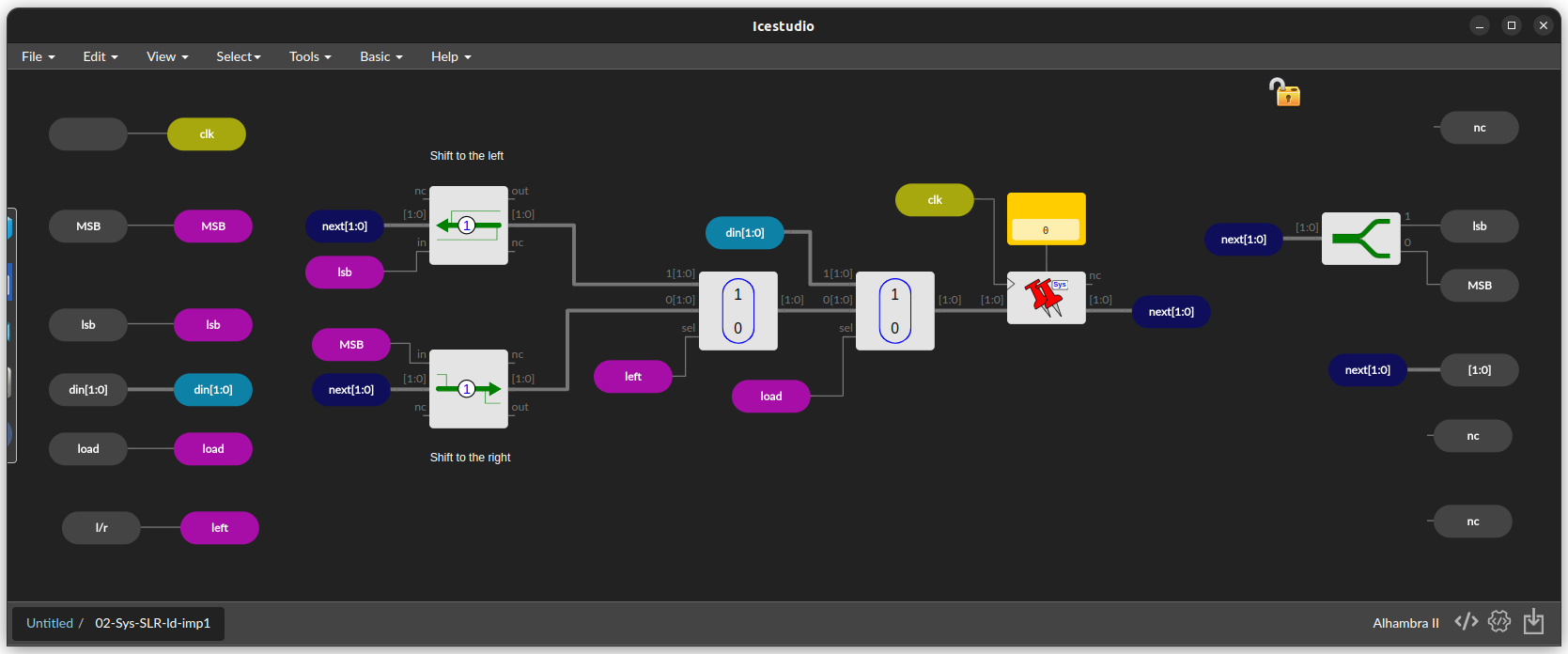
This is an implementation using only Icestudio blocks (no verilog code). The 2 bits Sys-SLR-ld-rst block is implemented from a 2-bits system registers with reset, a Combinational Shift right block, a Combinational Shift left block and a 2-bits 2-1 multiplexer

The system register is all the time capturing data from its input. The Mux is in charge of selecting which data is going to be loaded: either the external data or the shifted value. This selection is controlled by the load signal. When it is 1, the Mux select the external data (d input). When it is 0, the shifted data (sdata) is used instead
More information about these blocks in the following links:
- Iceswires collection: Combinational Shift block
- IceReg collection: system registers
- IceMux collection: Muxes
This is an implementation using only Icestudio blocks (no verilog code). The 2 bits Sys-SLR-ld-rst block is implemented connecting two system DFFs with reset in cascade
The reset signal is connected directly to the reset input of the Systems DFFs. The load is connected to the 2-1 muxes select input, so that they can either load the external value (load=1) or the shifted one (load=0)
This implementation is equivalent to the other two previous implementations
The standard shift left right register (SLR) or simply shift left right register shifts its N-bits value one bit to the left or right when its shift input is active. If one cycle pulse is applied to this input, the value is shifted 1-bit to the left or right depending on the input lr. If the shift input remains active, it behaves exactly the same as the system shift left right register (Shifting the value on every clock cycle)
As the shifting is controlled by the shift input, it allows us to shift the data at any rate of speed less than (or equal to) the system clock. Therefore these are the shift registers used for implementing serial transmiter/receivers with configurable speed

When shifting to the right (lr=0), the Most significant bit (MSB) is read from the MSB input. When shifting to the left (lr=1) the Least significant bit (lsb) is read from the lsb input. The top blue arrows indicate that this register can perform shifts in both directions
This is the verilog implementation of the 2-bits SLR block

The verilog code is shown below:
//-- Generic Shift Left/Right
//-- System register
//-- Number of bits
localparam N = 2;

//-- Initial value
reg [N-1:0] qi = INI;

always @(posedge clk)
begin

  //-- Shift left/right
  if (shift)

    if (lr == 0)
      //-- Shift to the right
      qi <= {MSB_i,qi[N-1:1]};

    //-- lr == 1
    else
      //-- Shift to the left
      qi <= {qi[N-2:0], lsb_i};
end

//-- Serial out:
//-- Least significant bit
assign lsb_o = qi[0];

//-- most significant bit
assign MSB_o = qi[N-1];

//-- Paralell out
assign q = qi;This is an implementation using only Icestudio blocks (no verilog code). The 2 bits SLR block is implemented from a 2-bits register with load, a Combinational Shift right block, a Combinational Shift left block and a 2-bits 2-1 multiplexer

More information about these blocks in the following links:
- Iceswires collection: Combinational Shift block
- IceReg collection: Registers
This is an implementation using only Icestudio blocks (no verilog code). The 2 bits SLR block is implemented connecting two DFFs in cascade. This implementation is equivalent to the other two previous implementations

The Shift Left Right register with reset (SLR-rst) works exactly the same as the SLR: it shifts the register value one bit to the left or right when the shift input is 1. But it includes the rst input for setting the register to its initial value (The one set in their Init top parameter)

When shifting to the right (lr=0), the Most significant bit (MSB) is read from the MSB input. When shifting to the left (lr=1) the Least significant bit (lsb) is read from the lsb input. The top blue arrows indicate that this register can perform shifts in both directions
This is the verilog implementation of the 2-bits SLR-rst block

The verilog code is shown below:
//-- Generic Shift Left/Right
//-- register with reset
//-- Number of bits
localparam N = 2;

//-- Initial value
reg [N-1:0] qi = INI;

always @(posedge clk)
begin

  //-- Reset
  if (rst == 1)
    qi <= INI;

  //-- No reset
  else

    //-- Shift left/right
    if (shift)

      if (lr == 0)
        //-- Shift to the right
        qi <= {MSB_i,qi[N-1:1]};

      //-- lr == 1
      else
        //-- Shift to the left
        qi <= {qi[N-2:0], lsb_i};
end

//-- Serial out:
//-- Least significant bit
assign lsb_o = qi[0];

//-- most significant bit
assign MSB_o = qi[N-1];

//-- Paralell out
assign q = qi;
The reset signal has the highest priority. When reset is 1, the register is loaded with its initial value. If reset is 0 then the shift input is checked. It will shift to the right if it is set (and reset is 0)
This is an implementation using only Icestudio blocks (no verilog code). The 2 bits SLR-rst block is implemented from a 2-bits registers with reset, a Combinational Shift right block, a Combinational Shift left block and a 2-bits 2-1 multiplexer

More information about these blocks in the following links:
- Iceswires collection: Combinational Shift block
- IceReg collection: Registers
This is an implementation using only Icestudio blocks (no verilog code). The 2 bits SLR-rst block is implemented connecting two DFF with reset in cascade. This implementation is equivalent to the other two previous implementations

The Shift Left Right register with load (SLR-ld) works exactly the same as the SLR: it shifts the register value one bit to the left or right when the shift input is set. But it includes the load input for loading the external value located in its data input (d) (It is also called parallel input)

The load signal has the highest priority. When it is active (1), the register does not perform the shifting. The shifting is done when the shift input is 1 and the load is NOT active (0)
This is the verilog implementation of the 2-bits SLR-ld block

The verilog code is shown below:
//-- Generic Shift Left/Right
//-- register with load
//-- Number of bits
localparam N = 2;

//-- Initial value
reg [N-1:0] qi = INI;

always @(posedge clk)
begin

  //-- Load
  if (load == 1)
    qi <= din;

  //-- No load
  else

    //-- Shift left/right
    if (shift)

      if (lr == 0)
        //-- Shift to the right
        qi <= {MSB_i,qi[N-1:1]};

      //-- lr == 1
      else
        //-- Shift to the left
        qi <= {qi[N-2:0], lsb_i};
end

//-- Serial out:
//-- Least significant bit
assign lsb_o = qi[0];

//-- most significant bit
assign MSB_o = qi[N-1];

//-- Paralell out
assign q = qi;
The load signal has the highest priority. When load is 1, the register is loaded with the external data. If load is 0 then the shift input is checked. It will shift to the right if it is set (and load is 0)
This is an implementation using only Icestudio blocks (no verilog code). The 2 bits SLR-ld block is implemented from a 2-bits registers, a Combinational Shift right block, a Combinational Shift left block and a 2-bits 2-1 multiplexer

More information about these blocks in the following links:
- Iceswires collection: Combinational Shift block
- IceReg collection: Registers
- IceMux collection: Mux 2-1
This is an implementation using only Icestudio blocks (no verilog code). The 2 bits SLR-ld block is implemented connecting two DFFs in cascade with two 2-1 Muxex. This implementation is equivalent to the other two previous implementations

The Shift Left Right register with load and reset (SLR-ld-rst) works exactly the same as the SLR-ld, but it includes the reset input for restoring the initial value

The reset signal has the highest priority. When it is active (1), the register loads its initial value. The load signal has the next priority. It only works if reset is not active. Finally, the less priority is for the shift signal. It only works if both reset and load are inactive
This is the verilog implementation of the 2-bits SLR-ld-rst block

The verilog code is shown below:
//-- Generic Shift Left/Right
//-- register with load and reset
//-- Number of bits
localparam N = 2;

//-- Initial value
reg [N-1:0] qi = INI;

always @(posedge clk)
begin

  //-- Reset (higher priority)
  if (rst == 1)
   qi <= INI;

  else

    //-- Load
    if (load == 1)
      qi <= din;

    //-- No load
    else

      //-- Shift left/right
      if (shift)

        if (lr == 0)
          //-- Shift to the right
          qi <= {MSB_i,qi[N-1:1]};

        //-- lr == 1
        else
          //-- Shift to the left
          qi <= {qi[N-2:0], lsb_i};
end

//-- Serial out:
//-- Least significant bit
assign lsb_o = qi[0];

//-- most significant bit
assign MSB_o = qi[N-1];

//-- Paralell out
assign q = qi;
This implementation shows clearly the signals priority: the high priority por the reset signal, then load and shift with the lowest priority
This is an implementation using only Icestudio blocks (no verilog code). The 2 bits SLR-ld-rst block is implemented from a 2-bits registers with reset, a Combinational Shift right block, a Combinational Shift left block and a 2-bits 2-1 multiplexer

More information about these blocks in the following links:
- Iceswires collection: Combinational Shift block
- IceReg collection: Registers
- IceMux collection: Mux 2-1
This is an implementation using only Icestudio blocks (no verilog code). The 2 bits SLR-ld-rst block is implemented connecting two DFFs with reset in cascade with two 2-1 Muxex. This implementation is equivalent to the other two previous implementations

The circuits used for testing all que components of this collection can be found on this collection:
- IceSRegs-TB: Testbenches for the Shift Registers. It is intended for developers, not for final users
All the component of this collection have been created from templates by python scripts Each family of shift registers has its on Template and Generation script:
| Component: Shift Right registers | Block identifier | Template | Python Script |
|---|---|---|---|
| System shift right register | Sys-SR |
Template-Sys-SR.ice |
generate-sys-sr.py |
| System shift right register with reset | Sys-SR-rst |
Template-Sys-SR-rst.ice |
generate-sys-sr-rst.py |
| System shift right register with load | Sys-SR-ld |
Template-Sys-SR-ld.ice |
generate-sys-sr-ld.py |
| System shift right register with load and reset | Sys-SR-ld-rst |
Template-Sys-SR-ld-rst.ice |
generate-sys-sr-ld-rst.py |
| Shift right register | SR |
Template-SR.ice |
generate-sr.py |
| Shift right register with reset | SR-rst |
Template-SR-rst.ice |
generate-sr-rst.py |
| Shift right register with load | SR-ld |
Template-SR-ld.ice |
generate-sr-ld.py |
| Shift right register with load and reset | SR-ld-rst |
Template-SR-ld-rst.ice |
generate-sr-ld-rst.py |
| Component: Shift Left registers | Block identifier | Template | Python Script |
|---|---|---|---|
| System shift left register | Sys-SL |
Template-Sys-SL.ice |
generate-sys-sl.py |
| System shift left register with reset | Sys-SL-rst |
Template-Sys-SL-rst.ice |
generate-sys-sl-rst.py |
| System shift left register with load | Sys-SL-ld |
Template-Sys-SL-ld.ice |
generate-sys-sl-ld.py |
| System shift left register with load and reset | Sys-SL-ld-rst |
Template-Sys-SL-ld-rst.ice |
generate-sys-sl-ld-rst.py |
| Shift left register | SL |
Template-SL.ice |
generate-sl.py |
| Shift left register with reset | SL-rst |
Template-SL-rst.ice |
generate-sl-rst.py |
| Shift left register with load | SL-ld |
Template-SL-ld.ice |
generate-sl-ld.py |
| Shift left register with load and reset | SL-ld-rst |
Template-SL-ld-rst.ice |
generate-sl-ld-rst.py |
| Component: Shift Left Right registers | Block identifier | Template | Python Script |
|---|---|---|---|
| System shift left right register | Sys-SLR |
Template-Sys-SLR.ice |
generate-sys-slr.py |
| System shift left right register with reset | Sys-SLR-rst |
Template-Sys-SLR-rst.ice |
generate-sys-slr-rst.py |
| System shift left right register with load | Sys-SLR-ld |
Template-Sys-SLR-ld.ice |
generate-sys-slr-ld.py |
| System shift left right register with load and reset | Sys-SLR-ld-rst |
Template-Sys-SLR-ld-rst.ice |
generate-sys-slr-ld-rst.py |
| Shift left right register | SLR |
Template-SLR.ice |
generate-slr.py |
| Shift left right register with reset | SLR-rst |
Template-SLR-rst.ice |
generate-slr-rst.py |
| Shift left right register with load | SLR-ld |
Template-SLR-ld.ice |
generate-slr-ld.py |
| Shift left right register with load and reset | SLR-ld-rst |
Template-SLR-ld-rst.ice |
generate-slr-ld-rst.py |
In this example it is shown how the System shift right registers from 2 to 32 bits are created from the template
This is the command line that should be executed within the Template folder:
obijuan@Hoth:~/Develop/Icestudio-collections/iceSRegs/Templates
$ python3 generate-sys-sr.py
This is the result:

If you need to modify the registers, open the corresponding template with Icestudio, edit the component (typically changing its verilog code) and save it
Then, you should generate the new registers with the corresponding script
The collection can be translated to any language. Any translation is very welcome!! 😀️ If you want to translate it to your native languaje please follow these instructions: Translating the collection into your language. This instructions are for the iceK collection, but the translation procedure is the same for any other collection
![]()
The Organization of this collections is exactly the same than all the other collections. It consist of the following folders:
-
blocks: This is were the icestudio blocks are located, with all the elements of the collection, organized by subfolders -
examples: Circuit examples ready to use in Icestudio. Inside this examples there are some special elements:-
00-Index.ice: Collection index. Here you will see some of the more important blocks that the collection contains
-
-
icons: Here you will find the SVG files for the icons used in the collection blocks. You can edit them or create new icons from them-
block+icon: Some of the blocks in SVG, for using them in your documentations. These are some examples:
-
-
locale: Folder with the English texts and their translation into other languages -
wiki: Images used in this wiki -
Templates: Generation scripts and Icetudio Templates
This is the Index file:
- 00-Index.ice:

Contributions are welcome! 😀️
You can contribute in different manners:
- Adding new blocks
- Translating the collection to your language
- Migrating the examples to more boards
These are the steps to follow for contributing:
- Fork the iceSRegs repo into your github account
- Clone it to your computer
- Install the collection as an external collection, so that you can access it from icestudio (See: Other uses: External collection)
- Create your own block
- Save it and click on Tools/Collection/Reload for using it and testing it
- Commit and push to your repo
- Emit a pull request
-
The main language is English: Create all your blocks and examples in English (the English text should be inside de .ice files). Then translate it to your local language (if you like), following the instructions mentioned here: Translating the collection into your language
-
The iceSRegs collection is ONLY FOR SHIFT REGISTERS. If you want to contribute with other type of blocks, do it in its corresponding collection (iceK, iceGates, iceRegs, iceCoders, iceFF...)
